

Multi-Layer Ceramic (MLC)
MLC
Due to the increase in the number of pins and the shrinking of the spacing between the horizontal probe card and the vertical probe card, the load capacity of the original circuit board has been exceeded, and a substrate must be added between the vertical probe card circuit board and the probe to deal with it. The ceramic substrate is aimed at higher substrate strength to overcome the expansion of the number of needles and DUT.
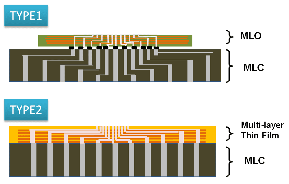
Depending on the design structure, NTK provides a complete circuit board, MLO, and Multi-Layer Ceramic (MLC).
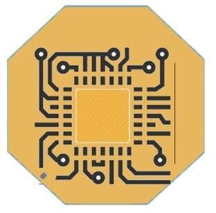
MLC Substrate
MLC Carrier
Why are ceramic substrates used?
High hardness
Directly bearing the pressure of the probe test and causing no deformation or damage on the ceramic surface PAD.
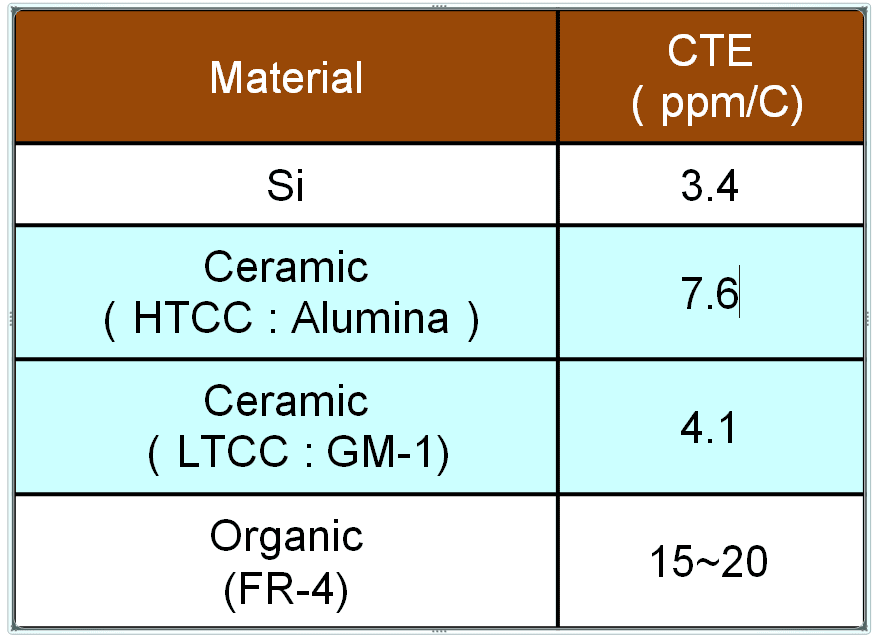
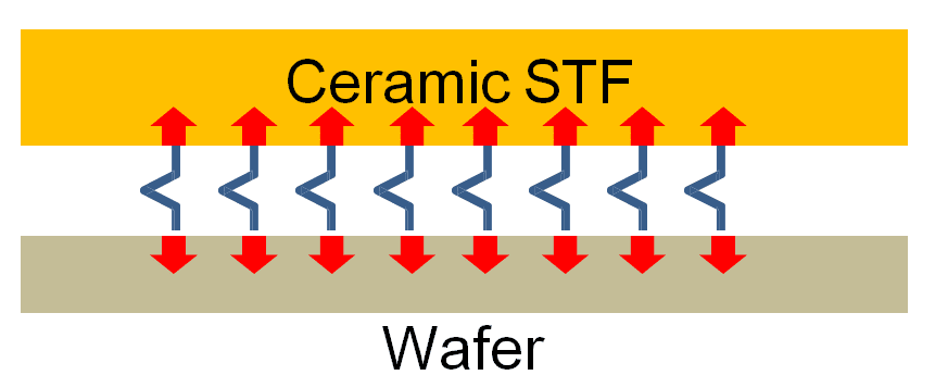
Low thermal expansion rate
Compared with organic materials, the thermal expansion rate of the board is closer to the thermal expansion rate of the wafer (silicon). In the high and low temperature test, the probe will not be unable to contact the wafer at the correct position due to the difference in the expansion rate.
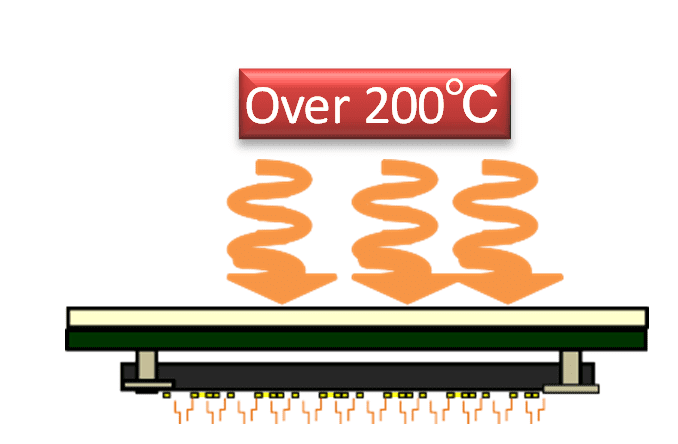
Heat resistance
Ceramics are high-temperature sintered materials. The sintering temperature is close to 800~1200 degrees. In the most severe wafer test, the shape and physical and electrical properties of the ceramic substrate can be maintained at an environment above 200 degrees.