

Printed wire board (PWB) is applied to probe card for IC test.
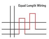
The complexity and electrical requirements of probe card design can be realized by PWB technology. Relying on the impedance control achieved by highly accurate and equal-length line layout, the accuracy of transmission time is improved with low signal interference.
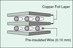
The use of pre-insulated copper wirse for wiring design on the board.
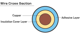
With stable electrical characteristics due to the consistent output of the pre-insulated copper wire diameter.
Compared with the etched circuit board, the theoretical value and the measured value are relatively consistent, so it is easy to achieve the required characteristics.
Due to the characteristics of wiring design and easy design changing, it is suitable for probe card in high density wiring.
MWB can realize the interleaving of circuit signals on the same layer, so the number of wires that can be routed in a single layer is significantly increased. Therefore, the manufacture of high-density wiring boards can be achieved in a smaller number of layers compared to traditional etching and plating boards. In addition, in MWB, insulated copper wires are used. The diameter of each line is the same as that of the same line. It can produce stable electrical characteristics such as accurate impedance control. The MWB line design is optimized by the program and the length is more suitable for circuit boards for high-speed signal switching. Compared with traditional etching circuit boards with limited manufacturing process, MWB is easier to complete manufacturing consistent with design values.
data original from Hitachi chemical